Metasurface, which consist of nanopillars with dimensions of hundreds of nanometers, has powerful ability of arbitrarily manipulating the optical field. However, how to make simulation results into real devices, is a difficult problem that “architects” need to explore. A qualitied metasurface device requires tens of iterations including Electron beam lithography (EBL), atomic layer deposition (ALD), reaction ion etching (RIE), etc, and also requires repeated experiments by “architects”.
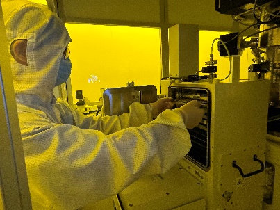
Figure 1. Electron beam lithography (EBL) experiment.
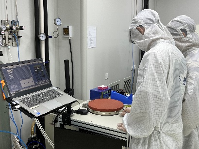
Figure 2. Atomic layer deposition (ALD) experiment.
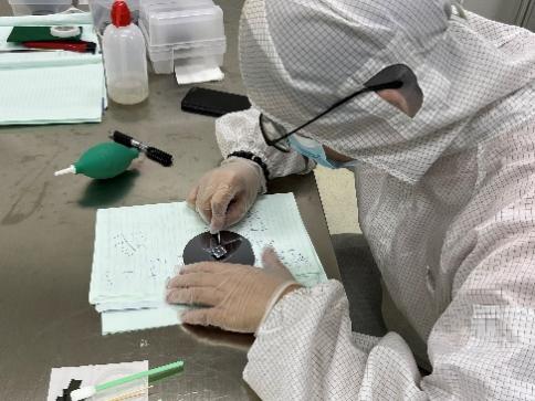
Figure 3. Reaction ion etching (RIE) experiment.
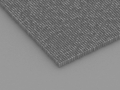
Figure 4. Fabrication result of a metasurface device.