
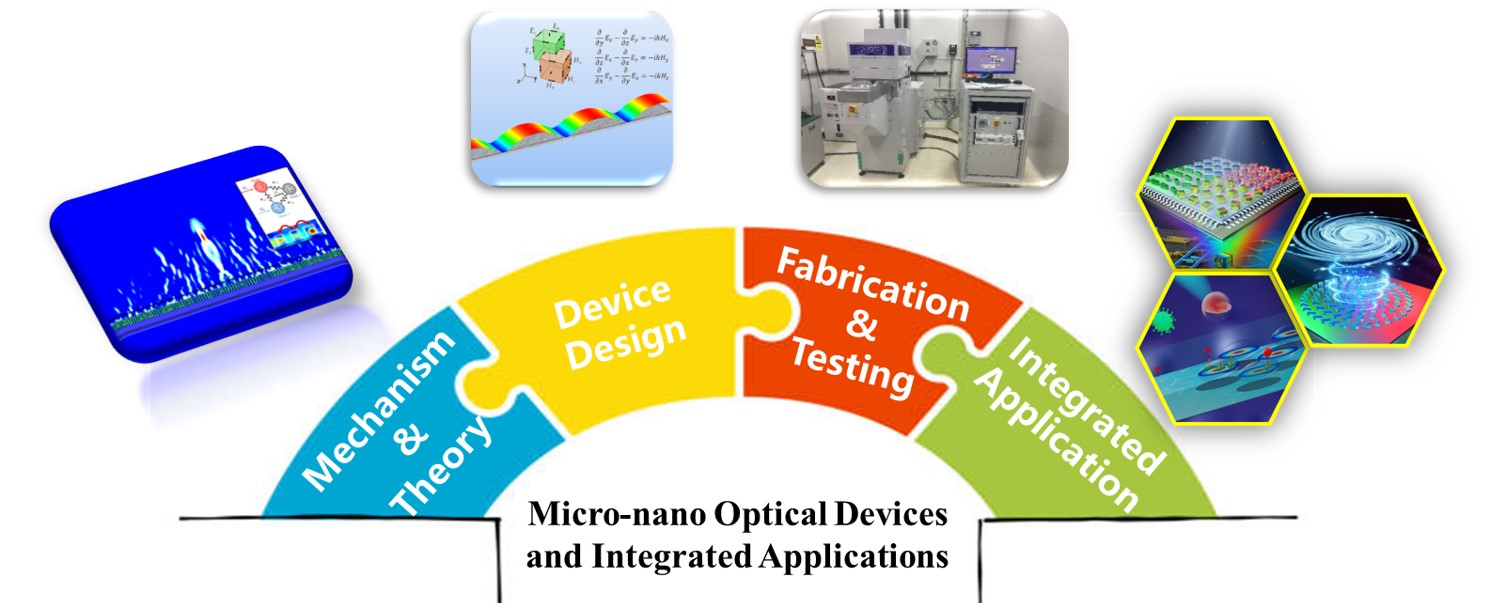
This division is devoted to the study of the regulation mechanism, device design, characteristic fabrication, and integrated applications of wafer-level micro-nano optical devices. The research direction focuses on theories of optical field modulation, computational electromagnetism, micro-nano machining technology, and on-chip integration applications.
By virtue of the “artificial microstructure”,the multi-dimensional optical field modulation can be achieved in micro-nano optics, including the amplitude, phase, polarization, and wavefront, which significantly surpasses capabilities with natural materials. Therefore,researches at the micro-nano level are considered a vital branch of optics. Micro-nano optical devices not only promote the thinning and integration of optical systems, but also significantly empower the advancement of intelligent sensing technology, which is one of the key strategical areas of national interest in China. However, the unclear modulation mechanism of micro-nano optics, inaccuracy of cross-scale device manufacturing, low precision in optical detection, and insufficient system design capabilities have limited the usability of micro-nano optical equipment.To overcome the aforementioned bottlenecks,researches regarding the fundamental theory, device design, preparation and characterization, and integrated applications have been conducted.

Regarding theoretical research and device design, the modulation mechanism of the optical field has been explored, as well as the computational theories of dimension reduction on an expanded eigenmode, and the system simulation of combining the calculations of the Fourier-space and real space have been developed. In addition, a full-wave simulation software of the three-dimensional electromagnetic field has been independently developed, which can improve the efficiency of computation and simulation of the optical field and remove the bottleneck in simulating micro-nano devices of mixed sizes.
Regarding the preparation and characterization, the research has been focused on the cross-scale manufacturing of micro-nano optical devices based on the electron beam lithography. The mechanism of error generation and calibration method in electron beam lithography have been elaborated. In addition, a dynamic write field exposure mode for nanostructures and large-aperture devices of different characteristic dimensions has been developed, which demonstrates the cross-scale manufacturing of micro-nano optical devices witha50 × 50 mm2aperture in the country.
Regarding applications, with excellent capabilities in micro-nano optical design,preparation and characterization, the promotion of on-chip photonics, on-chip multi-dimensional sensing, and optofluidic tweezing chips have been research focuses, aiming to achieve breakthroughs in the performance and application of micro-nano optical devices. Elaborated research areas have studied spectral imaging and intelligent sensing, optofluidic tweezers, on-chip integrated optical modulation, and computation. Artificial micro-nano superstructure and spectral imaging technology have been devised to accurately facilitate target measurement and identification in real-time. A new generation optofluidic tweezing chip has been developed, which can conduct the multi-functional ultra-precision modulation and measurement of miniature biological particles. Accordingly, this achievement can contribute to numerous significant biomedical applications. In addition, the interaction mechanism between the microstructure and optical field on nano-optical chips has been investigated to achieve on-chip dynamic optical modulation and computing.

©2022 Institute of Precision Optical Engineering TechnologyBeijingicp bei 05051632-16
Copyright: Institute of precision optical engineering technology, Tongji University
Tel: +86-21-65984652
Address: 1239 Siping Road, Shanghai, P.R. China
E-mail: 1986jiangli@tongji.edu.cn

