In recent years, the study of light–matter interactions and quantum processes at the nanoscale, such as polaritons, moiré physics, and topological phenomena, has attracted extensive attention. Traditional optical microscopy techniques are constrained by the diffraction limit, making it difficult to resolve the spatial heterogeneity and dynamic features of light–matter interactions at subwavelength scales. This limitation has significantly hindered progress in fundamental research and technological development. As a result, developing optical microscopy techniques that can overcome the spatiotemporal constraints of physical phenomena has become an important research direction.
The emergence of scanning probe microscopy, such as Atomic Force Microscopy (AFM) and Scanning Tunneling Microscopy (STM), has opened new avenues for surpassing the diffraction limit. By integrating these techniques with optical systems, near-field optical microscopy with atomic-scale resolution has been achieved. With the introduction of ultrafast pump–probe techniques, researchers have further realized simultaneous observation at nanometer spatial scales and femtosecond temporal scales.
Prof. Tao Jiang and Prof. Di Huang from the team of Prof. Zhanshan Wang and Prof. Xinbin Cheng at the School of Physical Science and Engineering, Tongji University, in collaboration with Prof. Markus B. Raschke from the University of Colorado at Boulder and Assistant Prof. Vasily Kravtsov from ITMO University in Russia, have provided a comprehensive overview of three representative ultrafast near-field optical microscopy techniques: Ultrafast scattering-type scanning near-field optical microscopy (Ultrafast s-SNOM), Ultrafast nanofocusing, and Ultrafast scanning tunneling microscopy (Ultrafast STM). They detail the working principles of these techniques and highlight their practical applications in ultrafast nano-spectroscopy and nano-imaging, covering the dynamic characterization and analysis of van der Waals materials, organic molecules, and various composite materials in terms of their electrical, mechanical, and magnetic properties. Finally, they summarize the current technological landscape from spatial, temporal, and spectral perspectives. They also explore the technical challenges and opportunities revealed by these applications and offer an outlook on future developments in the field.
This review titled "Applications of ultrafast nano-spectroscopy and nano-imaging with tip-based microscopy" was published in the high-impact SCI journal eLight. Paper link: https://doi.org/10.1186/s43593-024-00079-1
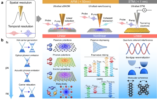
Figure 1: Ultrafast nano-spectroscopy and nano-imaging. a, Schematic illustration of the three types of ultrafast near-field optical microscopy discussed in this review. b, Representative physical processes investigated using ultrafast near-field optical microscopy, organized according to their characteristic timescales.
Highlights of the review
Ultrafast s-SNOM
Ultrafast s-SNOM is a versatile technique compatible with a wide range of detection wavelengths and materials. It has been widely applied to probe the dynamics of light–matter interactions at the nanoscale. Ultrafast s-SNOM typically uses a tapping-mode AFM tip illuminated by ultrafast laser pulses to excite local electric fields at the tip–sample interface. By employing a lock-in amplifier to demodulate the scattered light signal modulated by the tip oscillations, the technique enables access to the near-field optical response within a localized region beneath the tip. Recent technological advances have enabled ultrafast s-SNOM to drive a series of important breakthroughs in the dynamical study of polaritons, quantum phases, polarons, and many-body interactions.
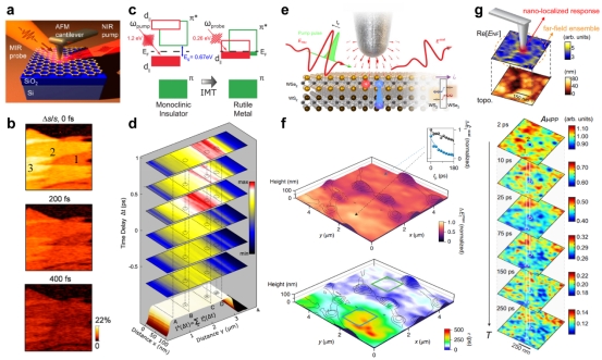
Figure 2: Probing nanoscale spatial heterogeneity using ultrafast s-SNOM. a–b, Spatiotemporal variations of plasmonic responses in graphene with different layer numbers. c–d, Correlation between the insulator-to-metal transition dynamics and spatial positions in VO₂ microcrystals under strong pump excitation. e–f, Exciton dynamics in a WSe₂/WS₂ heterostructure, correlated with the AFM topography. g, Study of many-body dynamics in perovskites under strong pump excitation.
Ultrafast nanofocusing
As an emerging technique, ultrafast nanofocusing addresses the limitations of ultrafast s-SNOM in studying nonlinear optical responses and offers femtosecond-level temporal resolution. Unlike conventional ultrafast s-SNOM, ultrafast nanofocusing utilizes a metallic tip integrated with a grating structure to efficiently couple ultrafast laser pulses into surface plasmon polaritons, which subsequently propagate and converge at the tip apex, forming a nanoscale localized ultrafast femtosecond light source. Through pulse shaping, this localized source not only provides sufficient intensity to support nonlinear optical studies but also enables coherent detection. Moreover, this approach significantly minimizes background signals that typically arise from direct illumination of the sample in traditional near-field techniques. To date, ultrafast nanofocusing has successfully enabled nanoscale coherent optical measurements such as second-harmonic generation, four-wave mixing (FWM), and anti-Stokes Raman scattering, offering unique advantages for investigating nanoscale coherent dynamics.
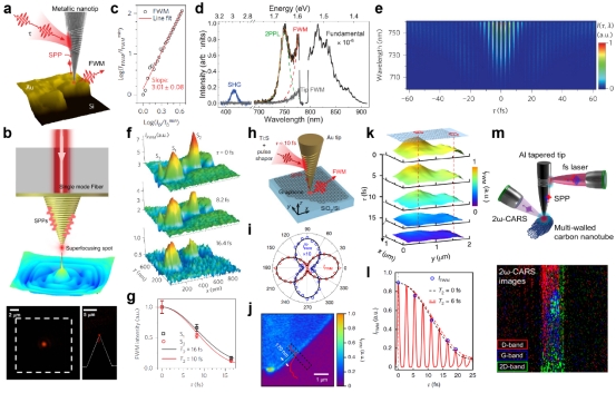
Figure 3: Applications of ultrafast nanofocusing in nonlinear nano-imaging. a-b, Schematic illustration of two types of ultrafast nanofocusing, with direct incidence of ultrafast pulses onto the grating structure of a metal tip and nanofocusing achieved by coupling light through an optical fiber. c, Relationship between the FWM signal generated by nanofocusing and excitation intensity. d, Spectra measured on monolayer WSe₂ using ultrafast nanofocusing. e, FWM interference spectra from the nanofocusing tip. f-g, Ultrafast FWM imaging performed on a nanostructured gold surface, with analysis of the dephasing time differences at different positions. h-j, Ultrafast nanofocusing characterization of graphene, including investigation of the polarization responses of the FWM signal and FWM imaging of the graphene. k-l, FWM imaging of graphene at different time delays, with analysis of the dephasing dynamics at the edge. m, Coherent anti-Stokes Raman scattering imaging of multi-walled carbon nanotubes by ultrafast nanofocusing.
Ultrafast STM
Ultrafast STM, which operates based on the principle of electron tunneling and incorporates ultrahigh vacuum and cryogenic techniques, achieves sub-ångström spatial resolution and stands as one of the most advanced microscopy methods available. In this technique, ultrafast laser pulses illuminate the STM tip, where the enhanced electric field at the apex modulates the tunneling junction between the tip and the sample, introducing an ultrafast optical-frequency component into the tunneling current. By demodulating the tunneling current signal, ultrafast STM simultaneously attains atomic-scale spatial resolution and temporal resolution comparable to the laser pulse width. Ultrafast STM has played an irreplaceable and critical role in advancing the study of electronic behaviors in both conventional and quantum materials. Moreover, the introduction of carrier-envelope phase control has further enabled precise coherent manipulation of the quantum process of electron tunneling.
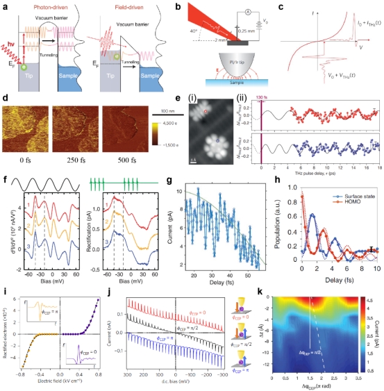
Figure 4: Spatio-temporal-spectrally resolved dynamics demonstrated by ultrafast STM and coherent manipulation of tunneling processes. a, Schematic illustration of the electron tunneling mechanism in a tunneling junction. b, Schematic of terahertz scanning tunneling microscopy (THz-STM). c, Nonlinear relationship between tunneling current and bias voltage in a tunneling junction. d, Autocorrelation measurements by THz-STM on a gold nanoisland placed on highly ordered pyrolytic graphite. e, Investigation of the coherent molecular dynamics of pentacene and copper phthalocyanine molecules. f, Inelastic electron tunneling spectra (left) and terahertz rectification spectra (right) of a hydrogen molecule located between the copper nitride surface and the tip. g, Ultrafast STM measurements on a gold nanorod exhibiting localized surface plasmon resonances. h, Coherent interference between the highest occupied molecular orbital and the surface states. i-k, Manipulation of the tunneling current by carrier-envelope phase modulation.
Prof. Xinbin Cheng and Prof. Tao Jiang from Tongji University, together with Prof. Markus B. Raschke from the University of Colorado at Boulder, served as co-corresponding authors. Zhichen Zhao, a Ph.D. student at Tongji University, is the first author of this review. Other authors who made significant contributions include Prof. Zhanshan Wang and Prof. Di Huang from Tongji University, along with Assistant Prof. Vasily Kravtsov from ITMO University in Russia.